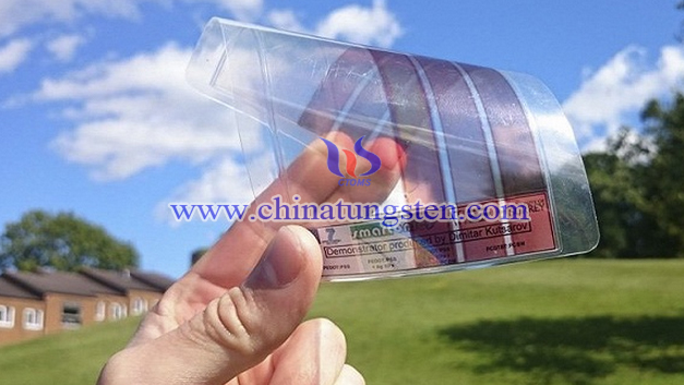
Application of Monolayer Tungsten Disulfide Film in Photoelectric Field
Two dimensional transition metal chalcogenide (TMDCs) is considered as a potential star material for future applications of electronic devices because of its graphene like structure.
The current research more semiconductor materials are tungsten disulfide WS2, molybdenum disulfide MoS2, MoSe2 molybdenum selenide, WSe2 tungsten selenide and so on. Among them, WS2 has the most promising application in electronic devices because of its bipolar electron transport properties.
Single layer two W is a kind of layered material similar to graphite with a layer spacing of 0.7 nm. WS2 is an important photoelectric material. When WS2 is changed from bulk material to single layer, the material changes from indirect bandgap to direct band gap semiconductor, and the band gap will change from 1.3eV to 2.0eV, which makes the monolayer tungsten disulfide thin films have important potential applications in photoelectric detectors and solar cells.
Monolayers of tungsten disulfide films show excellent performance in photodetection device research. Some scholars have found that based on 10-layer thick WS2 thin-film optical transistor devices, has the ability to detect monochromatic light of different wavelengths. When the wavelength is 514 nm, the photoresponse time of the device is about 5.3 MS, and the photoresponse rate is about 10 times of that of the MoS2 film.

In the field of solar cells, tungsten disulfide has shown great potential due to its excellent light response and absorption characteristics, some scholars have constructed ITO /WS2 /Au Schottky solar cells. The test results show that visible photocurrent can be produced under visible light irradiation. They also studied the effects of single layer, double layer and multilayer graphene electrodes on Al/WS2/rGO, Schottky cells. The results show that the Schottky contact between graphene and WS2 film is easy to form, so that the built-in electric field is formed at the interface between graphene and WS2 film, the photoinduced electron flows from the WS2 film to the Al electrode, and the hole flows from the WS2 film to the graphene, the maximum photoelectric conversion efficiency of the solar cell is up to 3.3%.
At present, the mass production of single-layer tungsten disulfide film is still difficult, the finished product quality is unstable and the cost is also high, this may be that tungsten disulfide is not as famous as graphene main surface. In the future, it is still a difficult problem for scientists to find a cheap and large area continuous preparation method of WS2 film and guarantee the quality and quantity.
If you have any inquiry of tungsten, please feel free to contact us:
Tel.: +86 592 5129696/+86 592 5129595
Fax: +86 592 5129797
Scan QR code of Chinatungsten Wechat platform to follow up the daily latest price and market of tungsten, molybdenum and rare earth.


评论
发表评论